
• 6 Posts
  • 9 Comments
Joined 1 year ago
cake
Cake day: June 17th, 2023

help-circle

  • DC motors have high inductance, meaning that the current going over it will resist to change. When you turn off a pair of nmos, current will likely start flowing over the the other pair, from source to drain. Depending on the spec of your nmos, you may consider using diodes in parallel to nmos to carry this current. Obviously these diodes should be reverse biased during normal operation.
  • As you said before power on capacitor is discharged. Right after power on capacitor is still discharged, so voltage on capacitor is zero, so reset pin has Vcc. With time capacitor gets charges and voltage across capacitor increases and reset voltage becomes closer and closer to ground, until it is ground. But it is important to consider what happens at power down too. At power down capacitor is charged. If power source becomes high impedance at power down, then reset pin will probably go down to zero in time but may take a bit time depending on what source exactly does. But if power source is connected to zero at power down reset pin will observe minus vcc and slowly go up to 0. If reset pin is sensitive it may be a good idea to protect it with a diode.


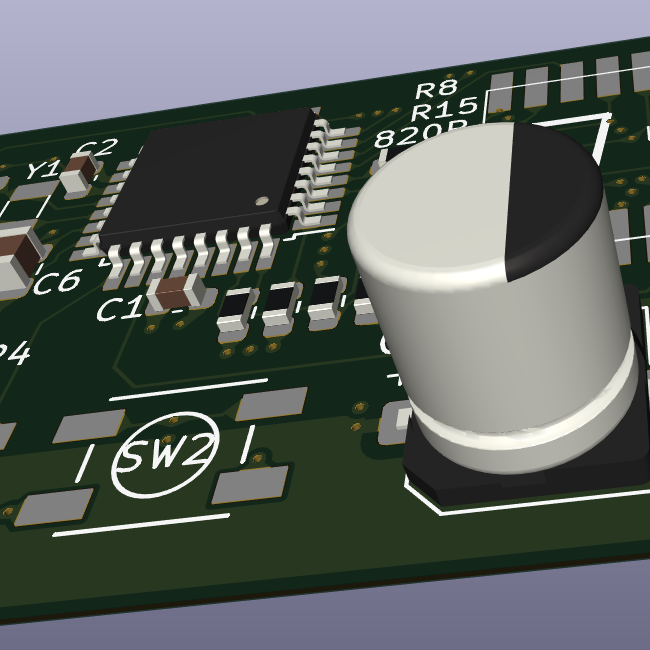
  • Depending on the power consumption, you may consider not using thermal relief while connecting thermal vias for the chip (component 57) to ground layers. But this may make soldering harder so do it only if needed. Thermal vias are so close that they form 3 long dents in 3v3 plane. It is good practice to put vias a little far apart so that planes can go through between vias. This can be important since sometimes lowest impedance can be obtained when current is flowing between those vias. If you don’t need to fit 15 vias there, you may consider reducing the number and separating them a bit. You can also check the design rules for minimum copper width and minimum via clearance for your manufacturer and enter them in your CAD tool.


  • I worked on asic verificationin sweden and i know that there are great opportunities. IC manufacturing became very expensive for lower manufacturing nodes and hence the tooling. It is not sustainable to have IC manufacturing facilities anymore unless you have very high volumes. So you can find only a handful places that perform state of the art IC manufacturing. But this doesn’t mean that you cannot work on IC, many companies does design and verification of their core functionality themselves if not the whole chip and outsource manufacturing and sometimes physical design to one of the big companies who specialized on this. To add this, there are areas that will make your transition to ee easier, if you choose to. Writing embedded software or working or test and verification usually requires more software skills than hardware and rf knowledge. Also try to keep a wide set of skills and don’t deep dive into a niche as it isn’t very certain what may vet automated in future. AI is getting very good at layout and physical design, which may limit pcb design or physical chip design opportunities in future. Not letting software go completely might be a good bet.